Table of Content
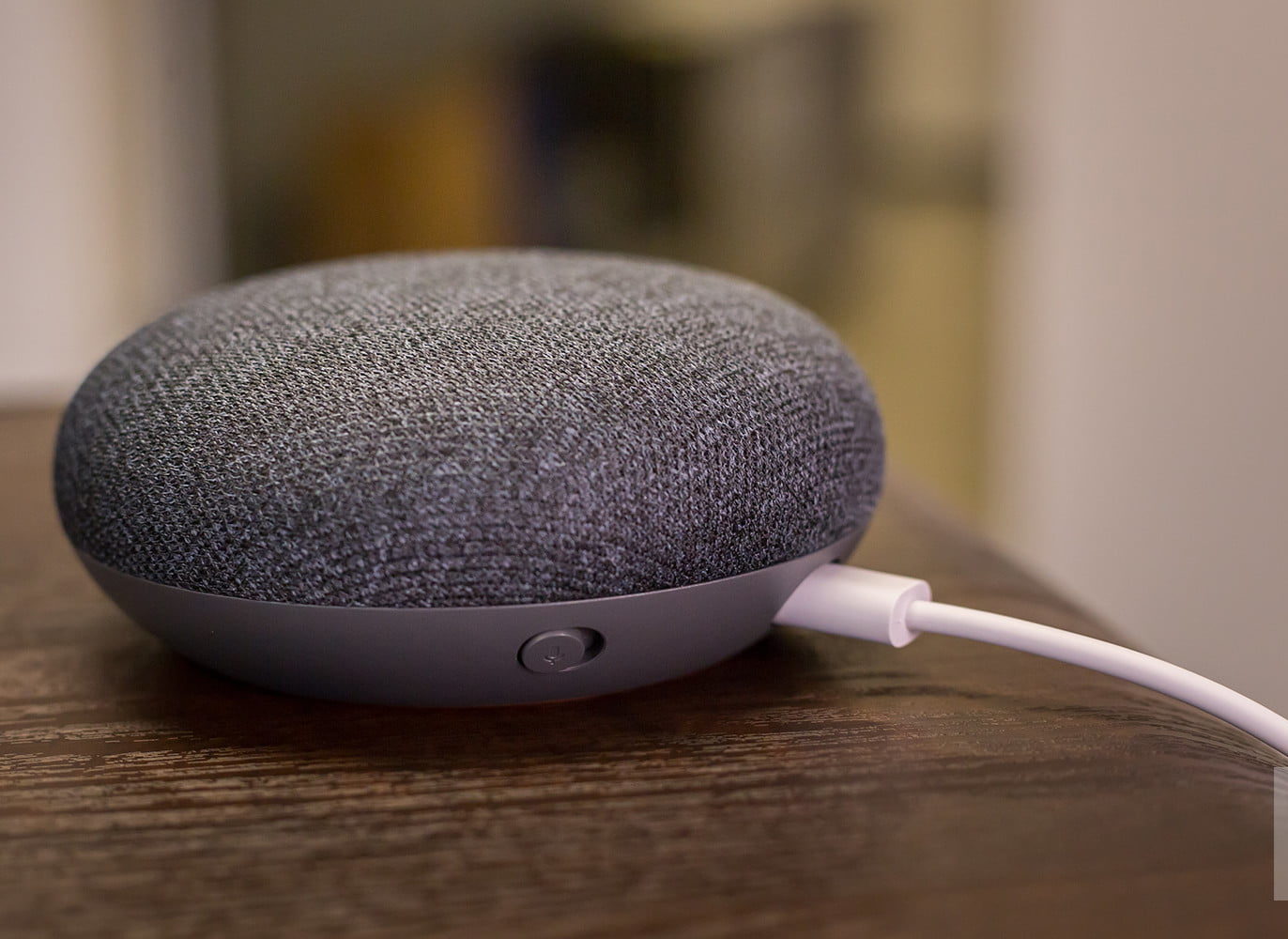
The five screws securing this piece, which covers the logic board, are not. If you forget the positions, the picture has your back. Four more T6 screws secure the speaker assembly to the front. The DC-in port is soldered to the motherboard, but is unlikely to experience much wear, considering the device stays plugged in. The stretchy o-ring seems to be the key to delving even deeper inside this smart speaker. Removing the base gives us our first look at that high-excursion speaker and a hidden micro-USB debug/programming port.
I cannot tell if it directly disconnects the microphone. While keeping the device close to the device as in the picture, first disconnect the ribbon cable from the connector with a spudger. One minor but interesting bit about the teardown was that there was what iFixit called a “mystery cable” with four contact points inside the part of the speaker that hold the magnets for its bottom case. The team came up with its own funny theories about this discovery, but what do you think this cable was made for? IFixit has posted its teardown of the Google Home speaker, revealing it to be easy to repair along with a mystery cable inside. Below you can see a line-up of their most significant internals.
Teardowns
These changeable imprints are built into the tools so that one can easily and reliably track parts that are made. Note the overmolded metal part has a resolution of down to the day (day 2 & 3 of week 33) corresponding to what I believe is the 14 & 15th August. The plastic overmolding however indicates the 13th August. Is there something I am missing, or did tight production schedules require time travel? It also looks like the white plastic base was manufactured a month later, in September, likely due to the stricter cosmetic requirement meaning it was iterated on during validation runs more than internal parts.
According to iFixit, getting to it is near-impossible due to the hefty, robust dollop of adhesive between it and the enclosure. So instead of redundantly tackling this same challenge myself, I’m going to “throw in the towel” and use iFixit’s images instead. Below are the specifications for Google Nest and Home speakers and displays . These are some common tools used to work on this device. Now lets take a look at the capacitive-touch volume controls, which did seem to be behaving.
Google Nest Hub Max
There is some seriously serious adhesive holding this board to the upper case. After turning the device over, you can gently lift the fabric-covered top. This guide will show you how to open the Google Home Mini and disassemble the individual components.
The fences still have large surfaces (providing a surface for the vacuum pick-up assembly method we discussed earlier) that we’ll need to cut away to identify all the chips. No long term harm here, as the shield covers will still protect from any noise once replaced. @hk_asking The switch is on a small peripheral board connected by a ribbon cable.
Smart home lighting: The hardware
I suspected that Google was clearing out existing inventory, either in preparation for a Nest rebrand or a more comprehensive next-generation replacement. I was able to snag one for $29 at Office Depot before inventory was depleted. But I’m suspicious of the placement of the contact on the PCB. You can see it was squeezed in quite close inbetween a foam gasket meant to reduce LED light spillover — which was resultingly trimmed shorter to make space, and the shield of the SDRAM — which one would not want to accidentally contact. Also, some adhesive conductive mesh was stuck over the gold-plated contact. This could be an attempted fix of a potential bad connection of the sheet metal to the PCB in the case of some tolerance misalignment or spring fatigue.

Also included is some Marvell switched-mode power supplies. There are also now only 4 RGB status LEDs, compared to the 12 in the original Google Home, and so they also got away with using only one LED driver, the NXP PCA9956BTW, instead of two. Ah, the pretty, soft-touch, and expressively-colored base-plate. Relieved of its T6s, the last piece pulls away with a bit of thermal shmoo.
Google Home Mini (1st gen)
Here is one I prepared earlier 👨🍳Removing the adhesive and the torx screws now allows the two halves of the product to easily come apart, revealing a ribbon cable that needs to be unplugged before completely seperating. This reveals what looks like a custom speaker enclosure attached with another 4 torx screws to the fabric shell. Underneath the rectangular lid there’s a Samsung K4B4G16 4 Gbit DDR3 SDRAM. And as previously mentioned, next to both of them is the Texas Instruments TAS5720 class D audio amplifier. Interestingly, across most of the molded parts, you can see dates of manufacturer.
I’m open to learn about how this compares in terms of time and cost on the assembly line. The flex cable connects to a small interfacing PCB, with a USB header, a toggle switch , and a reset button on the reverse, intended to be pressable through the baseplate. No other components here besides a decoupling capacitor for the 5V power supply. Overall, iFixit gave the speaker an 8 out of 10 on its own repairability scale, stating that it uses standard screws and connectors and that many of its parts are modular so they can be replaced quickly. The only low mark was given to the large amount of adhesive tape that was used to stick the touch board to the upper case of the Google Home.
With most of the PCB components covered, we can move our attention to the source of an unfortunate bug, that caused some early devices to continuously listen to audio. The feature-turned-bug was a touch sensor that could be used trigger the device to start listening without having to say the magic “Ok Google” wake command. Note the thermal pad which helps conduct heat from the main processor, through the shield and to the metal “heat-sink”/speaker bracket.

We turn up the heat on this teardown and bust out some enhanced interrogation tools—an iOpener and dental pick to be exact. This cable runs from motherboard up to a board tucked in the top of the lid, probably home to a fancy microphone and LED array. Its an arm that goes between the mute button and its switch on the board, to give it just the right amount of springy resistance. The board is glued to 2 locations lightly, but can still be removed easily. If there is still glue over the screw heads you can easily pierce with the screwdriver. Do not remove glue, as the bottom will not hold otherwise later.
Using a plastic spudger, unfasten the zero insertion force connector latch. Slide the ribbon connector out of the ZIF connector to free it. To pull out the four Torx screws hiding deep in the speaker recess, we pull out our set of fixed-blade screwdrivers for a little extra reach. Back in May, I started noticing $70-off (the normal $99.99 list price, and also versus the original $129.99 MSRP) promotions for Google’s first-generation Home smart speaker at various retailers.
Below you can see the capacitive touch sensor consisted of stamped sheet metal adhered onto the inside of the plastic shell, surrounding the LED light pipes. A small, gold tipped spring contact was used to connect to the PCB. The purpose of the black-and-red two-wire twisted pair is likely already obvious to you; it heads inside the chassis and (I’m quite confident, though I haven’t yet confirmed at this point in the teardown) connects to the speaker on the other end. The flex PCB cable headed toward the bottom, on the other hand, stay tuned. Peeling back some adhesive foam, you can see a flex cable soldered directly to the board — marginally cheaper but significantly tougher than the ZIF connector used on the other end of the cable.
There have been a lot of teardowns of the Dot done so be sure to check them out if you’d like to learn more of the details. On initially hearing that the controls required tapping, I thought this might have been done by an accelerometer, which we can see it wasn’t. If cheap enough, this may have actually helped provide the redundancy necessary to eliminate false positives on the capacitive touch sensors, but hindsight is 20/20. One can see the gold-plated tip of the stainless-steel is to connect with the golden contacts visible on the PCB.


No comments:
Post a Comment